Memory, memory addressing & structure
Memory
Memory forms an important part of any computer system, as it is used to temporarily store data and programs that are being utilised by the microprocessor. Two types of memory are used these are ROM and RAM.
ROM (Read Only Memory)
ROM contains programs and data that is required by the microcomputer at start up. The contents of ROM cannot be changed, under normal conditions. The programming of ROM is done at the manufacturing stage. ROM is split into further types, these are:
PROM Programmable Read Only Memory
EPROM Erasable Programmable Read Only Memory
EEPROM Electrically Erasable Programmable Read Only Memory
A PROM is basically ROM that has not been programmed. The programming is done by the user, by using a special PROM programming unit. Once programmed the PROM cannot be reprogrammed.
The EPROM may be reprogrammed, in the same way as the PROM, but only after the contents have been erased. This is done by subjecting the microchip to ultra violet light for 40 to 45 minutes.
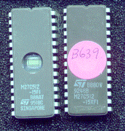
Eproms
EEPROM allows the reprogramming to be done without having to erase the previous memory contents.
ROM chips on the motherboard, may contain the BIOS (Basic input/output System), the initialisation routines for the microcomputer system, diagnostic routines, the routine for handling the diskette boot procedures, system configuration and BASIC (Beginners All-purpose Symbolic Instruction Code) interpreter. In most cases the POST (Power On Self Test) is also included.
Other uses for ROM on the motherboard are to store programs that run directly on power-up, such as dedicated word processing and proprietary control software.
ROM has a disadvantage in that the memory access is generally slow, in comparison to RAM. This has lead to some manufacturers programming the BIOS to copy the ROM into RAM on start-up, providing an improvement in performance. This “SHADOW” RAM is however lost to the operating system as a result.
Flash eprom technology had already been used for network adapters in the early nineties. It soon became the norm for motherboards, allowing BIOS upgrade from a floppy disk. Some 80486 motherboards had this as an additional feature with most Pentium motherboards having it as standard. Pentium II,III and IV all have this feature as standard.
Further recent extensions to this technology are of course the “flash memory” cards now (2005) used almost exclusively by cameras and phone-cameras.
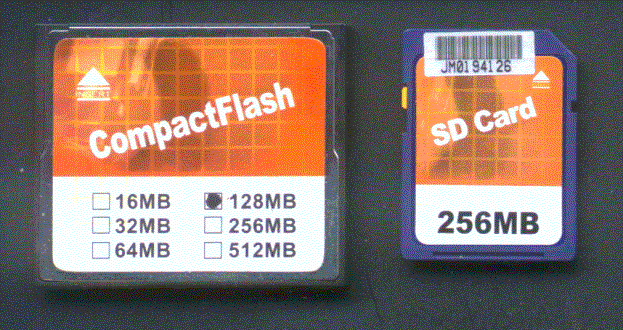
Compact flash and Secure Digital memory cards
RAM (Random Access Memory)
RAM is split into 2 further types, these are SRAM (Static Random Access Memory) and DRAM (Dynamic Random Access Memory). RAM generally has faster access than ROM, however RAM has the disadvantage of being volatile. That is: when power is removed from static or dynamic RAM, the contents disappear.
Dynamic RAM uses small capacitors mounted on a grid of lines. The capacitors hold a charge that signifies a binary 1. When RAM is read, the capacitors are automatically recharged. DRAM capacitors discharge fairly quickly (4mSec), so a refresh cycle is required to automatically recharge the small capacitors. The refresh is really a memory read on a block of cells, and this is done transparently by the memory refresh hardware many times per second.
Static ram uses transistor flip-flops that can store data for long periods of time, as long as power is supplied to the RAM chip. The access time for SRAM can be extremely fast. The CMOS (Complementary Metal Oxide Semiconductor) RAM that is used to store system information on 80286/80386/80486 systems is static ram. The content of the CMOS RAM is variable according to system set-up. The SRAM is used because the memory chip only requires a low level of power, and this can be supplied by a battery pack.
NOTE: Both ROM and RAM memory chips are sensitive to static electricity and to protect these components they should be carried in anti static tubes or containers.
Parity - Hardware error detection
In any sequence of bits, parity can be calculated on those bits according to even or odd parity. In the PC this is done by a hardware chip and stored into the ninth memory location. Should the bit generated by the parity check chip not correspond to the bit stored in the ninth bit, a parity alarm signal is generated. The parity alarm signal is connected to the Non Maskable Interrupt (NMI) line and produces the dreaded message "system parity error : system halted".
Where did this (hardware parity check) come from?
Why from here of course (the original IBM PC) ....
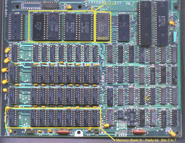
IBM PC Motherboard showing the memory area in detail.
This is the memory on an old IBM PC motherboard. It didn’t stay like that of course. The memory shown above was a maximum of 64k. Very quickly - in a matter of months - it was upgraded to 128k. As higher dynamic ram chips became available, the base capacity of the motherboard was increased. The clone motherboards very quickly overtook the IBM ones and reached 640k with two rows of 256k each and a single row of 128k.
AT motherboards usually came with 512k or 1024k of memory. Again with little room (board real-estate) for expansion. To increase the memory on these computers you would purchase an entension memory card with a lot of memory chips. These you would spend an hour or so fitting into the sockets and checking that there were no bent pins and they were in the right way round.
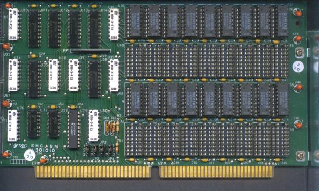
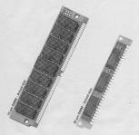
Memory card using dynamic ram chips.
(only half shown, it was a full length card!)
Clearly this memory took up a large amount of space and during this period chip manufacturers were making vast amounts of money. As the chip capacity took leaps and bounds so the size and area reduced.
The memory card shown above would consume a large percentage of the 5 Volt supplied. The power supply was uprated from the 130Watt for the PC/XT to 200 to 300Watts, depending on application. This consumption would create a fair amount of heat and a incredible amount of circulating currents in the printed circuit boards used. This current could easily be of the order of 400 Amperes! This circulating current being switched on and off by address accesses would cause a lot of RFI (Radio Frequency Interference). Interference that was not very well contained by the steel case. Whilst the machines were FCC classified so that they didn’t interfere with other computer equipment, medium/short wave reception in offices was usually out of the question.
With the advent of the 80386 we saw the smaller, lower current memory modules being used by virtually all the motherboards.
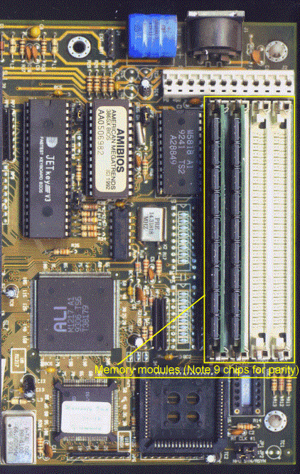
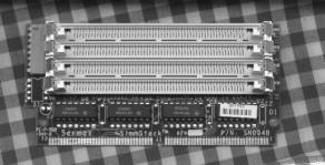
80386 Motherboard
showing the 30 pin memory modules and nine chips used for 8bits and 1 for parity checking.
Memory Modules
Memory modules started appearing with the later 80286 clones as the motherboard real-estate was reduced from the original large area board. Some single in-line modules used pins to plug in to sockets on the main board. But the majority used a single printed circuit board connector into an angled socket.
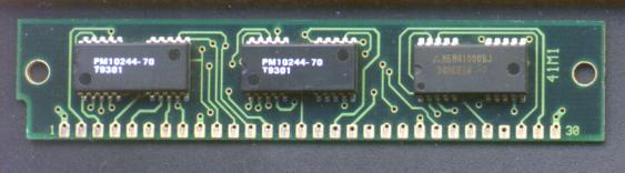
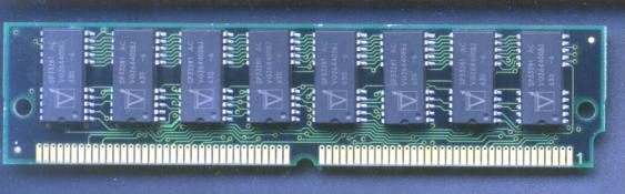
30 pin Memory Module (SIMM)
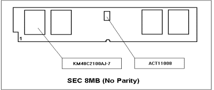
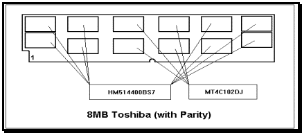
Unfortunately some SIMM (single in-line memory module) manufacturers made SIMMs with and without parity. This lead to problems, as you cannot mix the two types on a motherboard. You could disable parity checking if you have a late model motherboard, allowing both to be used.
How do you tell which SIMM has parity or hasn’t? Count the number of chips on the SIMM. If a SIMM has 9 chips or a multiple of 9 then it will have parity.
Mix-n-Match its not
Mixing SIMMS of different manufacturers is also a recipe for disaster, as access time differences will produce parity errors or worse, unexplained crashes. Similarly different construction SIMMs will produce errors. The OLD SIMMs would have nine 1M Bit chips on a SIMM, whereas the new variety have two 4 bit chips and a 1 bit parity chip. These cannot be mixed reliably in a machine.
72 pin and 30 pin SIMMs A ‘SIMM-VERTER’ allows you to use up those 30 pin SIMMs
72 pin Memory Module
Not covered here (for future addition to these notes)
Expanded and Extended memory. The Lotus/Intel/Microsoft standard.
EDO memory chips improved the performance of dynamic memory. Supported in 80486 and Pentium I systems.
SDRAM modules as used by Pentium II, III and early Pentium IV computers.
DDR memory as used in Pentium IV computers.
Memory Addressing
Each memory or port component in the PC has a unique address. A given I/O adapter may have both an I/O address and memory addresses. The memory addresses are for the memory on that card. For example, a VGA card has a given I/O address for the 6845 video controller, and the RAM on the card, used for the text and graphics, has a memory address.
The lowest memory addresses, below 640k are for motherboard RAM and are used to store the interrupt vector table, the BIOS data area, the DOS working area and the user’s programs.
An 8086 processor has 20 address lines resulting in the addressing of 1,048,576 bytes of memory. The 8086 having only 16 bit registers has to add two registers together to obtain the required 20 bits. This is done with a segment register and an offset register. The address in the offset register is offset 4 bits from the physical address and the two values are then added to obtain the physical address. This 20 bit address is then placed onto the address bus.
The 80386 and 80486 has 32 address lines and can address 4,294,967,296 bytes of memory in its virtual protected or native mode.
NOTE: Its called ‘real mode’ because the address specified in the segment and offset, actually refer to a physical address in memory.
CPU addressing - how it works. Byte addressing and Word addressing.
The 8088 had 16 bit registers and an external 8 bit data bus. The 8086, 80186 and 80286 all had 16 bit registers as well as 16 bit external data buses. This meant that these processors had an advantage of being able to transfer 16 bits at a time over the data bus, rather than two 8 bit bytes. This speeds up the retrieval of data from memory. With the 80386 and up this becomes 4 bytes per memory access. This all supposes that the data is aligned on either a word boundary or double word boundary. If it isn’t the cpu will have to have two or four retrievals to obtain the data. Compilers and assemblers can be instructed to place the data on word or double word boundaries, thus making programs perform better when a higher processor is used.
Intel Notation
The original 8080 (not 8088) processor stored its 16 bit words with the high byte in the higher memory location. This method has carried on throughout the Intel range of processors. Other manufacturers of processors, such as Motorola use the lower memory location for the highest byte. This leads to interesting data conversion problems between systems of different processors. If a 16 bit number is read from memory you will have to transpose the right byte value and the left byte to obtain the correct value. A 32 bit number is stored in a similar manner, with the highest byte of the four bytes, stored highest in memory.
Example: The pointers stored in the interrupt table are stored like this :-
|
[OFFSET] |
: |
[ SEGMENT] |
|
[low byte][high byte] |
: |
[low byte][high byte] |
Looking at Memory addresses with Debug
Debug has been provided with DOS since version 1.0. It provides a system monitor program which can be used for ‘debugging’ programs. For a detailed manual see the document DEBUG.txt.
Debug commands and functions include:
< Compare 2 blocks of a system memory
< Display contents of system memory
< Display and modify the content of system memory
< Fill the memory with data or data from a string
< Go and execute the program from an address.
< Specify break points in a program and display system status
< Load data from a diskette into memory
< Move the contents of memory from one location to another.
< Send data to an I/O port.
< Display the contents for the processor registers and flags.
< Search system memory for data specified in a string.
< Trace the execution of a program and display processor CPU status.
< Disassemble an assembly language program.
< Write a block of system memory to diskette.
Debug is a command driven program and as can quickly be seen, it was designed for programmers. The hyphen "-" is used as the prompt. To obtain some help, type a ? and press enter.
To examine a block of memory start DEBUG from the DOS prompt and after the "-" appears, type in D40:0 and press Enter. This will give a "D"ump of the memory at segment 40 hexadecimal in both hexadecimal and ASCII.
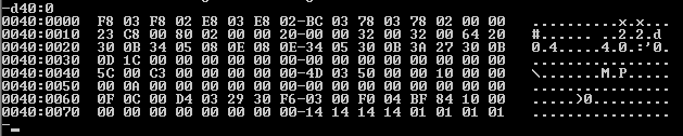
A memory address is a physical location within the total memory, at which data can be stored. Under DOS, memory is divided into segments each of which comprises 64 k of contiguous bytes of memory. An individual memory address within a segment is called an offset. The first byte in a segment is offset 0 the second is offset 1 etc. Individual memory addresses are identified by their segment address and offset. Debug knows nothing about extended memory and cannot be used to examine memory above 1MB.
The PC’s Memory Structure
The XT & AT System memory map
|
Decimal (k = 1024) |
Hexadecimal (absolute physical) |
Function |
|
960k |
FFFFF to F0000 |
64k system ROM BIOS, Power On Self-Test and possibly
BASIC. |
|
816k |
EFFFF to CC000 |
Reserved for ROM attachments on adapters. |
|
800k |
C0000 |
VGA ROM bios attachment |
|
736k |
B8000 |
CGA adapter display memory. |
|
704k |
B0000 |
Monochrome & Hercules adapter display memory. |
|
640k |
A0000 |
EGA / VGA adapter graphics display memory. |
|
1024 0000 |
9FFFF 004FF 00400 00000 |
DOS & USER memory (Read / Write memory.) BIOS DATA AREA Interrupt vector table |